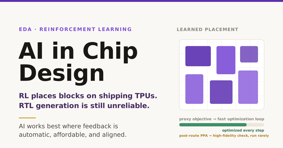
The chips that train and run modern AI are increasingly designed with help from AI. Reinforcement learning places the large blocks on Google's recent TPUs [1], a domain-adapted language model writes internal tooling scripts at NVIDIA [9], and the three largest EDA vendors have each shipped systems that run parts of the design flow while an engineer reviews the result. The gains are real, and they are concentrated where the design flow can evaluate a candidate automatically, cheaply enough to run the loop many times, and with enough fidelity to track the engineering result that matters. Describing a chip in plain English and getting correct hardware back is the application people imagine first, and it is the one that works least well today.
A short film I designed for this piece.
Why chip design became an AI problem
The economics forced the question. Designing a leading-edge chip is now a large capital commitment on its own, before a single wafer is manufactured. McKinsey put the end-to-end cost of a 5nm design at about 540 million dollars [22], and the widely cited IBS estimates place a 3nm design near 580 to 650 million and a 2nm design above 700 million [23]. These are model-based estimates rather than audited figures, and they vary by source and vintage, but the trend is not in dispute. Each new process node raises the cost of designing the chip, not only the cost of fabricating it.
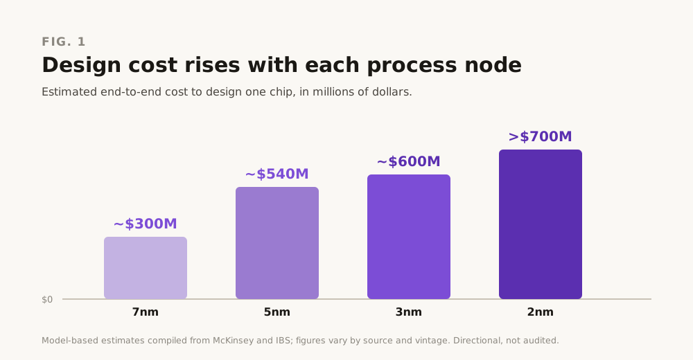 The cost of designing a chip, separate from the cost of manufacturing it, climbs with each node.
At the same time, the engineers who do this work are scarce. A 2023 study by the Semiconductor Industry Association and Oxford Economics projected that the United States semiconductor workforce would need to grow by roughly 115,000 jobs by 2030, and that about 67,000 of those positions risk going unfilled at current graduation rates [18]. Deloitte's global estimate is larger, more than one million additional skilled workers by 2030 [19]. A 2026 NSF workshop report on AI for electronic design automation puts the structural gap in blunt terms, counting roughly 1.8 million software developers in the workforce against about 78,000 hardware designers [25]. Demand is moving the other way. Every major hyperscaler now designs its own accelerators, from Google's TPU to Amazon's Trainium, Microsoft's Maia, and Meta's MTIA, and Broadcom has guided to a custom-silicon opportunity in the tens of billions of dollars by 2027 [20]. More chips, more complex chips, and not enough engineers to design them. That shortage is one reason the industry is turning to AI. Rising design complexity and the growing share of every schedule spent on verification are others.
What makes an EDA task amenable to AI
Electronic design automation, or EDA, is the software that carries a chip from a high-level description to a layout a foundry can manufacture. These tools automate the steps of the design flow and check each result before the next step begins.
A digital chip moves through that flow as a long pipeline. An architecture becomes register-transfer-level (RTL) code, usually Verilog or VHDL. The RTL is verified against a specification, synthesized into a gate-level netlist, placed and routed on the physical die, checked for timing and manufacturability, and finally taped out. Each stage has its own tools and its own failure modes.
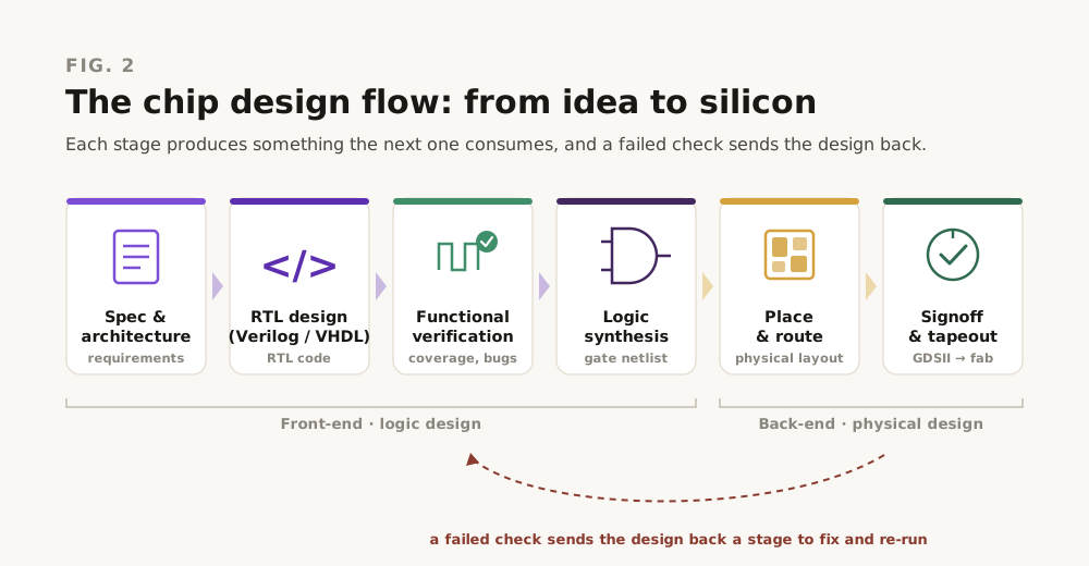 The digital design flow, from specification to tapeout. Each stage produces something the next stage consumes, and a failed check sends the design back to an earlier step.
AI does not help every stage equally, and the quality of the feedback at each stage predicts where it helps. For machine learning to improve fast, three things have to be true about how a candidate design gets scored. The score has to be automatic, so the loop can run without a person judging each attempt. It has to be affordable, cheap enough to compute that the search can run many times over. And it has to be aligned, tracking the engineering result that matters at the end rather than a convenient stand-in for it.
That last condition is the one that is easy to miss. When a cheap score poorly predicts the final timing, power, or functional correctness, an optimizer will improve the score while making the real chip worse. It optimizes the wrong thing, very efficiently.
Placement is the case where all three hold. During the search, a candidate layout is graded by fast proxies for wirelength, congestion, and density, which stand in for the routed power, timing, and area that matter more but are far slower to measure. Verification is similar: coverage metrics and reference models give an automatic, repeatable score, and a learning system can optimize against it many times over. A written specification of what a block should do is not a score of this kind. Nothing automatic tells you whether a block of generated Verilog matches the intent behind the English, which is why turning a description into correct RTL is still the hard part.
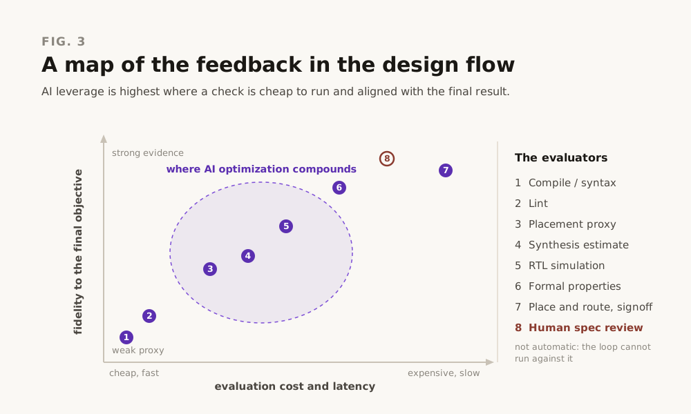 The band where a check is cheap enough to run in a loop and still tracks the final objective is where learning and search compound.
Optimization against a measurable objective
The clearest results are in physical design and implementation, where the task is to search for a layout that minimizes power, area, and timing violations.
Google's AlphaChip is the most visible example. The method treats macro placement as a sequence of decisions and trains a reinforcement learning agent, guided by a graph neural network, to position the large blocks on the die. During training the agent is rewarded by a fast approximate objective, a weighted proxy for wirelength and congestion, rather than by a full place-and-route and signoff of each candidate, which would be far too slow to run inside the loop. The original work appeared in Nature in 2021 [2]. In 2024 Google reported that the method had been used for the last three generations of its Tensor Processing Unit, including the v5e, v5p, and Trillium chips, and for its Axion data-center CPUs, and it released a pre-trained model and the training framework as open source [1]. The accelerators that train large models were themselves laid out in part by a learning system.
"With each new generation of TPU, including our latest Trillium (6th generation), AlphaChip has designed better chip layouts and provided more of the overall floorplan, accelerating the design cycle and yielding higher-performance chips."
Google DeepMind [1]
The adoption reaches beyond Google. MediaTek has reported extending the same method for its own production floorplanning:
"At MediaTek, we've been pioneering chip design's floorplanning and macro placement by extending this technique in combination with the industry's best practices."
SR Tsai, Senior Vice President, MediaTek [1]
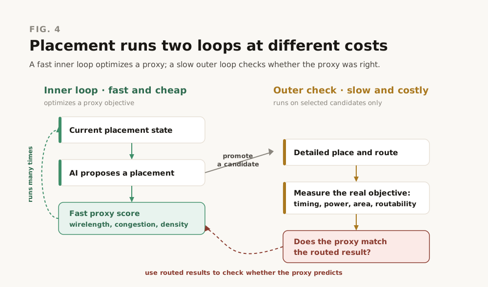 The inner loop is cheap enough to run many times; the outer loop is what tells you whether the proxy was measuring the right thing.
The commercial tools tell a similar story from the vendor side. Synopsys shipped DSO.ai in 2020 as an autonomous optimizer for the implementation flow, and by early 2023 reported it had crossed 100 production tapeouts, with aggregate results of more than 3x productivity and power reductions up to 15 percent [6]. Cadence's Cerebrus applies reinforcement learning to the same problem. It helps to separate the three kinds of claim Cadence makes for it. The broad product claim is a ceiling: up to 10x productivity and up to 20 percent PPA improvement [7]. Cadence's own worked example is narrower and more concrete. On a CPU block, Cerebrus reported 14 percent higher performance, 7 percent lower leakage, 3 percent lower total power, and 5 percent higher density, reached in about ten days of optimization by a single engineer [27]. Cadence separately reports a production full-flow migration in which Cerebrus improved total negative slack and reduced leakage power on a critical MCU design [7]. Siemens EDA's Aprisa AI reports comparable numbers, roughly 10x productivity and 10 percent better PPA on RTL-to-GDS implementation [8]. Every one of these figures comes from a vendor or its customer, measured on a workload the vendor chose, so treat them as directional rather than independently audited. What makes them credible is the consistency across three competitors and the fact that customers are taping out real parts with these flows.
Verification is where these methods pay off next. It takes more of a modern project's schedule than design does, and it comes with quantitative scores in coverage closure and bug detection. Synopsys VSO.ai reports up to 10x reduction in coverage holes in customer use, and Cadence's Verisium platform applies learning to root-cause analysis and debugging. This is unglamorous work, and it is exactly where a measurable objective makes machine learning pay off.
The AlphaChip dispute
AlphaChip is also a lesson in how to read claims in this field, so it deserves a direct account.
After the Nature paper, a group at UC San Diego led by Andrew Kahng published an assessment arguing that the reinforcement learning approach did not clearly beat a strong simulated-annealing baseline or commercial tools on their open benchmarks, and they questioned the reproducibility of the original results [3]. Igor Markov later published a sharper critique in Communications of the ACM [4]. That article now carries an ACM editorial expression of concern stating that an investigation is underway into the content and disclosure of the critique itself, so the critique is under scrutiny rather than settled. Google responded in detail, arguing that the critics had not run the method as published: they omitted the pre-training step, used a fraction of the compute, and stopped training early [5]. Nature examined the original paper and in September 2024 published an addendum that added methodological detail, including the use of initial block locations; critics maintain the addendum still lacked the full training and evaluation inputs needed for independent replication [2].
The most useful recent data point is a 2025 update from the UC San Diego group that addresses several of Google's main methodological objections. This time they fine-tuned from Google's released pre-trained checkpoint and routed the designs fully, rather than stopping at the training proxy, and they still found that reinforcement learning did not consistently outperform established placement methods and typically required significantly more compute to match them [26]. That result is worth holding next to the deployment record. Google reports learned placement across three TPU generations and its Axion CPUs, which are shipping products rather than benchmark tables, and MediaTek separately reports using the technique in its production floorplanning.
I am not going to settle that dispute here. Benchmark evidence and production evidence answer different questions. One asks whether the method beats the best alternative under controlled, equal-compute conditions, where the record is genuinely contested. The other asks whether experienced teams found it useful enough to put in real designs, where the answer appears to be yes. For a practitioner, the lesson is narrow. Before you believe a placement result from anyone, ask for the pre-training, the compute budget, the baseline, and whether the comparison used fully routed results or a proxy.
Language models and RTL
Generating hardware from a natural-language description is the most anticipated application and the least mature.
The appeal is clear. If a language model can turn a description into working Verilog, it multiplies the scarcest resource in the flow, senior RTL designers. NVIDIA's ChipNeMo is the most serious attempt to make this work inside a real design organization. It took Llama 2 models at 7B, 13B, and 70B, adapted the tokenizer to hardware vocabulary, continued pre-training on internal design data, and fine-tuned for three jobs: an engineering-assistant chatbot, EDA-script generation, and bug summarization [10]. The 70B model beat GPT-4 on two of those three tasks, and a 13B domain-adapted model matched the general-purpose 70B, which is a strong result for domain adaptation over raw scale [9]. Notice what those tasks are. They assist the work around the design, answering questions, drafting scripts, summarizing bugs. None of them generates the functional RTL that becomes the chip.
Direct RTL generation is where the honesty is needed. On the VerilogEval benchmark, capable general models reach roughly 60 to 65 percent pass rates on specification-to-RTL problems, and 2025 reasoning-tuned open models such as CodeV-R1 pushed single-attempt scores into the high 60s [11][13]. Those numbers look encouraging until you reach the harder, more realistic benchmarks. NVIDIA's 2025 CVDP benchmark, built from 783 problems spanning generation, verification, and debugging in both agentic and non-agentic form, found that the best available models reached no more than 34 percent pass@1 on code generation, and that the agentic verification tasks were the hardest of all [12]. The broader benchmark matters because it exposes failure modes that clean, self-contained generation tasks tend to hide. The same NSF workshop report found that current models "produce RTL designs that are riddled with a prohibitively large number of bugs for complex designs," which is why natural-language-to-RTL has not yet delivered the productivity gains its proponents expected [25].
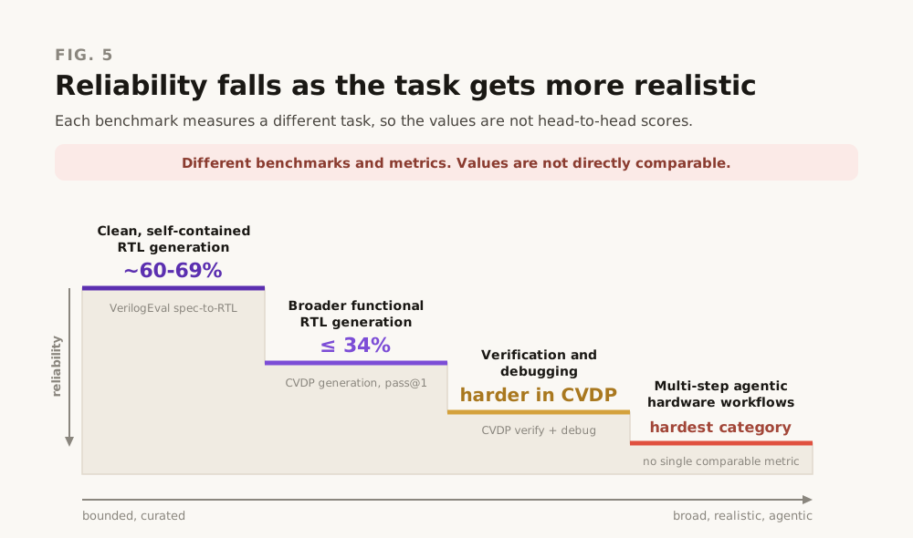 Reliability drops as evaluation moves from bounded RTL-generation problems toward broad, realistic hardware-engineering workflows. The numbers come from different benchmarks and are not directly comparable; see the references.
The failure modes are specific. Models produce syntactically valid Verilog that compiles and then fails functional simulation. They invent signals and constructs that do not exist. Take a small FIFO. A model can produce Verilog that compiles cleanly and passes a basic write-then-read test, and still mishandle the corner cases that matter: a simultaneous read and write when the buffer is nearly full, the pointer wraparound at the end of the address space, or the flag behavior on reset. A compile check catches none of this. A directed simulation catches some of it. Catching all of it takes assertions or formal properties that state what full, empty, and simultaneous access are supposed to mean. That progression, from a syntax check to simulation to formal properties to system-level verification, is a hierarchy of feedback, and each step costs more and tells you more. A cheap automatic check can tell you something useful long before it tells you enough. A generated design cannot be trusted until it has been verified, and verifying untrusted RTL is exactly the expensive step the generation was supposed to save. This is why the credible research direction pairs generation with testbench feedback, training the model against simulation results rather than against text. Simulation feedback improves generation because it evaluates functional behavior, where current models struggle much more than they do with syntax.
Agentic EDA closes the loop
The 2025 and 2026 product cycle reframed all of this as autonomous agents. Synopsys started with a generative copilot in 2023 [14] and then demonstrated AgentEngineer, a path from single-step assistants toward multi-agent flows, with large speedups reported on specific autonomous workflows [15]. Cadence acquired ChipStack and announced an AI Super Agent for front-end design and verification, with customers reporting up to 10x lower verification effort on selected blocks [16]. Siemens shipped its own agentic EDA system. The capital behind this signals how strategic the industry considers it: Synopsys closed a roughly 35 billion dollar acquisition of Ansys in July 2025 [21], and NVIDIA took a two-billion-dollar stake in Synopsys in December 2025 to accelerate these tools on its GPUs [17].
Cadence's chief executive is direct about what the agents now do:
"The agentic layer is also doing work that EDA never really did before, like writing RTL or generating verification code. This is augmenting the human capability."
Anirudh Devgan, CEO, Cadence [24]
There is a real technical reason this direction could matter. An isolated model turns a specification into RTL and stops. An agent connected to the tools runs a loop instead: it generates RTL, compiles it, simulates it, reads the failure, revises, runs lint and synthesis, checks timing, and repeats. The second setup is interesting not because it is agentic but because the model is now inside a closed loop, with the simulator and the checker supplying machine-readable engineering feedback at each step. That is the condition under which learning and search have paid off everywhere else in the flow. Whether today's agents close that loop reliably on production-scale designs is the open question, and it is why these systems are still presented as operating with engineering review and human sign-off.
I take the productivity numbers seriously and I discount them at the same time. They are vendor-reported, measured on workflows the vendor chose, and nearly every announcement carries the same qualification: a human engineer reviews and signs off on the agent's output. That is the correct design, not a flaw. But it means the agent compresses the work around a decision rather than making the decision, and the reviewing engineer still has to understand the hardware. The autonomy levels in these roadmaps are a real direction of travel. They are not yet a description of an unsupervised flow.
What this means from a systems perspective
This is a recurring pattern in my own work on hardware and software co-design. It holds because chip design already had the evaluators. When a candidate can be evaluated automatically, cheaply, and against the objective that actually matters, learning and search will use that signal relentlessly. When the only judge is a human reading a specification, you get fluent output that someone still has to check by hand.
Chip design is unusually rich in those signals. It has decades of investment in simulators, formal verification, reference models, timing engines, and quantitative PPA metrics. That accumulated verification infrastructure, more than the models themselves, is what makes AI effective here. The scale of that infrastructure is easy to underestimate. The same workshop report, drawing on long-running functional-verification surveys, notes that verification can consume up to 80 percent of design effort and that first-silicon success rates are at their lowest since 2004 [25]. It is also why the results cluster in placement, implementation, and coverage closure, and why natural-language-to-silicon lags. Those three come with automated evaluators that capture much of the objective. Natural-language-to-RTL does not come with one cheap, comprehensive test of whether the generated design captures the full intent of the specification.
For anyone deciding where to invest, this suggests a clear order. Adopt the optimization and verification tooling now, because the evidence is on the ground and the objective is measurable. Treat RTL generation as an assistant to senior engineers rather than a replacement, and budget for the verification it creates. And if you are building these tools, improving the evaluator can matter as much as increasing model capability. A cheaper and more trustworthy way to evaluate what the model produces is often what separates a demonstration from a part you can manufacture.
When a vendor or a paper puts a placement or generation result in front of you, a few questions separate a real result from a demonstration:
- What is the model actually optimizing, and is it the final engineering objective or a proxy for it?
- How well does that proxy predict fully routed timing, power, and area?
- What is the baseline, and did it get equal compute and equal engineering effort?
- Is the evidence a benchmark, a vendor evaluation, a customer case study, or shipping silicon?
- How much verification does the output create before anyone can trust it?
- What stays under human review, and what happens when the tool optimizes the wrong constraint?
- What does the evaluator fail to capture, and what would a failure hiding in that gap look like?
A related point sits underneath the talent-shortage framing. These tools make a competent engineer more productive and let an expert take on more, but they do not remove the need to understand what the hardware is doing. An agent that closes timing 30 percent faster only helps someone who can tell when it closed timing on the wrong constraint. That judgment does not become less valuable as the tools improve. I have made this argument about AI systems generally in my writing on hardware and software co-design and why AI engineers need to understand hardware, and chip design is now the sharpest version of it.
The chips that run AI are being designed, in part, by AI. The advance that made that possible was not only better generative models. It was connecting them to the decades of simulation, optimization, verification, and signoff infrastructure the field already had. In chip design, the evaluator is as important as the model. What none of this has done, and will not do soon, is remove the engineer who understands why a design is correct.
References
[1] Google DeepMind, "How AlphaChip transformed computer chip design," September 26, 2024.
[2] A. Mirhoseini, A. Goldie, et al., "A graph placement methodology for fast chip design," Nature 594, 207–212, June 9, 2021.
[3] C.-K. Cheng, A. B. Kahng, et al., "Assessment of Reinforcement Learning for Macro Placement," ISPD 2023.
[4] I. L. Markov, "Reevaluating Google's Reinforcement Learning for IC Macro Placement," Communications of the ACM 67(11), 60–71, October 23, 2024.
[5] A. Goldie, A. Mirhoseini, J. Dean, "That Chip Has Sailed: A Critique of Unfounded Skepticism Around AI for Chip Design," arXiv:2411.10053, November 15, 2024.
[6] Synopsys, "How AI-Driven EDA Tools Enhance Chip Design and Verification" (DSO.ai reaches 100 production tapeouts), February 7, 2023.
[7] Cadence, "Cadence Cerebrus AI-Based Solution Delivers Transformative Full-Flow Design Migration," Cadence Newsroom, June 9, 2022.
[8] Siemens, "Siemens turbocharges semiconductor and PCB design with AI" (Aprisa AI, Calibre Vision AI, Solido), June 23, 2025.
[9] NVIDIA, "Silicon Volley: Designers Tap Generative AI for a Chip Assist" (ChipNeMo), October 30, 2023.
[10] M. Liu, et al., "ChipNeMo: Domain-Adapted LLMs for Chip Design," arXiv:2311.00176, October 31, 2023.
[11] N. Pinckney, et al., "Revisiting VerilogEval: A Year of Improvements in Large-Language Models for Hardware Code Generation," arXiv:2408.11053, August 20, 2024.
[12] NVIDIA, "Comprehensive Verilog Design Problems (CVDP): A Next-Generation Benchmark Dataset for Evaluating LLMs and Agents on RTL Design and Verification," arXiv:2506.14074, June 17, 2025.
[13] Y. Zhu, et al., "CodeV-R1: Reasoning-Enhanced Verilog Generation," arXiv:2505.24183, May 30, 2025.
[14] Synopsys, "Synopsys Announces Synopsys.ai Copilot," November 15, 2023.
[15] Synopsys, "Synopsys Announces Expanding AI Capabilities for its Leading EDA Solutions" (AgentEngineer), September 3, 2025.
[16] Cadence, "Cadence Unleashes ChipStack AI Super Agent," February 10, 2026.
[17] NVIDIA, "NVIDIA and Synopsys Announce Strategic Partnership" (2 billion dollar investment), December 1, 2025.
[18] Semiconductor Industry Association and Oxford Economics, "Chipping Away: Assessing and Addressing the Labor Market Gap Facing the U.S. Semiconductor Industry," July 25, 2023.
[19] Deloitte, "The global semiconductor talent shortage," 2024.
[20] CRN, "AI Semiconductors, VMware Driving Broadcom to New Heights" (custom-ASIC serviceable-market guidance), June 6, 2025.
[21] Synopsys, "Synopsys Completes Acquisition of Ansys," July 17, 2025.
[22] McKinsey & Company, "Semiconductor design and manufacturing: Achieving leading-edge capabilities," August 20, 2020.
[23] IBS advanced-node design-cost estimates, as compiled in industry reporting (for example, Semiconductor Engineering), 2020–2022.
[24] More Than Moore, "Analyst Q&A with Cadence CEO Anirudh Devgan," April 15, 2026.
[25] J. Cong, D. Z. Pan, R. Puri, Y. Sun, et al., "Report for NSF Workshop on AI for Electronic Design Automation," arXiv:2601.14541, February 2026.
[26] C.-K. Cheng, A. B. Kahng, S. Kundu, Y. Wang, Z. Wang, "An Updated Assessment of Reinforcement Learning for Macro Placement," IEEE Transactions on Computer-Aided Design of Integrated Circuits and Systems, December 15, 2025.
[27] Cadence, "Cadence Cerebrus Intelligent Chip Explorer," Cadence Community (Breakfast Bytes), July 22, 2021.
Discussion
Sign in with GitHub to leave a comment or react. Threads are public and live in this site's GitHub Discussions.